- 您现在的位置:买卖IC网 > Sheet目录996 > NCP3066SCBCKGEVB (ON Semiconductor)EVAL BOARD FOR NCP3066SCBCKG
�� �
�
�NCP3066,� NCV3066�
�APPLICATIONS�
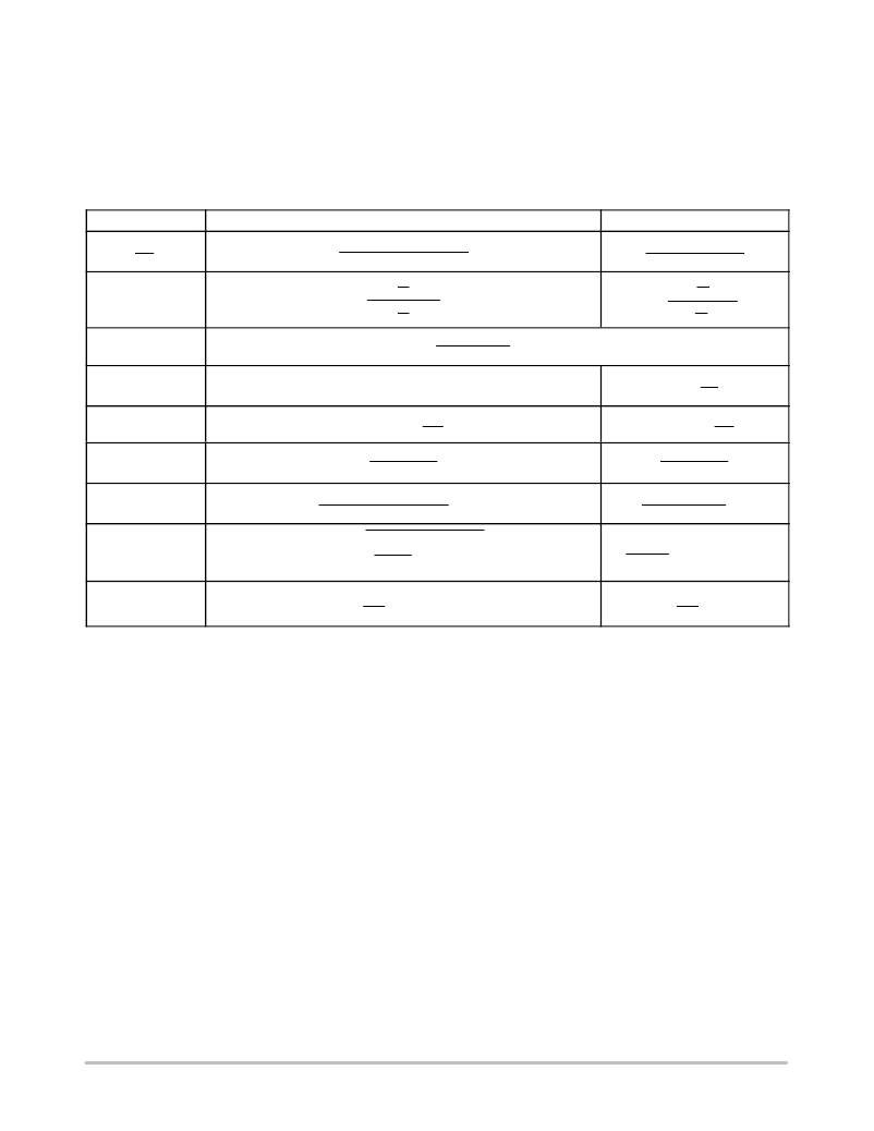
�Figures� 15� through� 24� show� the� simplicity� and� flexibility�
�of� the� NCP3066.� Two� main� converter� topologies� are�
�demonstrated� with� actual� test� data� shown� below� each� of� the�
�circuit� diagrams.� The� demo� boards� have� an� input� for� a� digital�
�dimming� signal.� You� can� provide� a� PWM� signal� to� change�
�the� average� output� current� and� reduce� the� LED� brightness.�
�Figure� 14� gives� the� relevant� design� equations� for� the� key�
�parameters.� Additionally,� a� complete� application� design� aid�
�for� the� NCP3066� can� be� found� at� www.onsemi.com.�
�Parameter�
�ton�
�toff�
�t� on�
�Step� ?� Down�
�Vout� )� VF�
�Vin� *� VSWCE� *� Vout�
�ton�
�toff�
�Step� ?� Up�
�Vout� )� VF� *� Vin�
�Vin� *� VSWCE�
�ton�
�toff�
�f�
�ton�
�toff�
�)� 1�
�f�
�ton�
�toff�
�)� 1�
�CT� +� 381.6� @� 10�
�C� T�
�f� osc�
�*� 6�
�*� 343�
�10� *� 12�
�I� L(avg)�
�Iout�
�Iout�
�ton�
�toff�
�)� 1�
�I� pk� (Switch)�
�IL(avg)� )�
�D� IL�
�2�
�IL(avg)� )�
�D� IL�
�2�
�R� SC�
�0.20�
�Ipk� (Switch)�
�0.20�
�Ipk� (Switch)�
�L�
�Vin� *� VSWCE� *� Vout�
�D� IL�
�ton�
�Vin� *� VSWCE�
�D� IL�
�ton�
�V� ripple(pp)�
�D� IL�
�1�
�8� f� CO�
�2�
�)� (ESR)� 2�
�ton Iout�
�CO�
�)� D� IL�
�ESR�
�I� out�
�V� ref�
�R� s�
�V� ref�
�R� s�
�9.� V� SWCE� ?� Darlington� Switch� Collector� to� Emitter� Voltage� Drop,� refer� to� Figures� 7� and� 8.�
�10.� V� F� ?� Output� rectifier� forward� voltage� drop.� Typical� value� for� 1N5819� Schottky� barrier� rectifier� is� 0.4� V.�
�11.� The� calculated� t� on� /t� off� must� not� exceed� the� minimum� guaranteed� oscillator� charge� to� discharge� ratio.�
�Figure� 14.� Design� Equations�
�The� Following� Converter� Characteristics� Must� Be� Chosen:�
�V� in� ?� Nominal� operating� input� voltage.�
�V� out� ?� Desired� output� voltage.�
�I� out� ?� Desired� output� current.�
�D� I� L� ?� Desired� peak� ?� to� ?� peak� inductor� ripple� current.� For� maximum� output� current� it� is� suggested� that� D� I� L� be� chosen� to� be�
�less� than� 10%� of� the� average� inductor� current� I� L(avg)� .� This� will� help� prevent� I� pk� (Switch)� from� reaching� the� current� limit� threshold�
�set� by� R� SC� .� If� the� design� goal� is� to� use� a� minimum� inductance� value,� let� D� I� L� =� 2(I� L(avg)� ).� This� will� proportionally� reduce�
�converter� output� current� capability.�
�f� ?� Maximum� output� switch� frequency.�
�V� ripple(pp)� ?� Desired� peak� ?� to� ?� peak� output� ripple� voltage.� For� best� performance� the� ripple� voltage� should� be� kept� to� a� low�
�value� since� it� will� directly� affect� line� and� load� regulation.� Capacitor� C� O� should� be� a� low� equivalent� series� resistance� (ESR)�
�electrolytic� designed� for� switching� regulator� applications.�
�http://onsemi.com�
�9�
�发布紧急采购,3分钟左右您将得到回复。
相关PDF资料
NCP5005GEVB
EVAL BOARD FOR NCP5005G
NCP5006EVB
EVAL BOARD FOR NCP5006
NCP5030MTTXGEVB
EVAL BOARD FOR NCP5030MTTXG
NCP5602EVB
EVAL BOARD FOR NCP5602
NCP5603GEVB
EVAL BOARD FOR NCP5603G HI FREQ
NCP5604AAGEVB
EVAL BOARD FOR NCP5604AAG
NCP5608EVB
EVAL BOARD FOR NCP5608
NCP5612GEVB
EVAL BOARD FOR NCP5612G
相关代理商/技术参数
NCP3066SCBSTGEVB
功能描述:电源管理IC开发工具 NCP3066 SOIC8 BOOST DB
RoHS:否 制造商:Maxim Integrated 产品:Evaluation Kits 类型:Battery Management 工具用于评估:MAX17710GB 输入电压: 输出电压:1.8 V
NCP308MT090TBG
功能描述:监控电路 RoHS:否 制造商:STMicroelectronics 监测电压数: 监测电压: 欠电压阈值: 过电压阈值: 输出类型:Active Low, Open Drain 人工复位:Resettable 监视器:No Watchdog 电池备用开关:No Backup 上电复位延迟(典型值):10 s 电源电压-最大:5.5 V 最大工作温度:+ 85 C 安装风格:SMD/SMT 封装 / 箱体:UDFN-6 封装:Reel
NCP308MT120TBG
功能描述:监控电路 RoHS:否 制造商:STMicroelectronics 监测电压数: 监测电压: 欠电压阈值: 过电压阈值: 输出类型:Active Low, Open Drain 人工复位:Resettable 监视器:No Watchdog 电池备用开关:No Backup 上电复位延迟(典型值):10 s 电源电压-最大:5.5 V 最大工作温度:+ 85 C 安装风格:SMD/SMT 封装 / 箱体:UDFN-6 封装:Reel
NCP308MT125TBG
功能描述:监控电路 RoHS:否 制造商:STMicroelectronics 监测电压数: 监测电压: 欠电压阈值: 过电压阈值: 输出类型:Active Low, Open Drain 人工复位:Resettable 监视器:No Watchdog 电池备用开关:No Backup 上电复位延迟(典型值):10 s 电源电压-最大:5.5 V 最大工作温度:+ 85 C 安装风格:SMD/SMT 封装 / 箱体:UDFN-6 封装:Reel
NCP308MT150TBG
功能描述:监控电路 RoHS:否 制造商:STMicroelectronics 监测电压数: 监测电压: 欠电压阈值: 过电压阈值: 输出类型:Active Low, Open Drain 人工复位:Resettable 监视器:No Watchdog 电池备用开关:No Backup 上电复位延迟(典型值):10 s 电源电压-最大:5.5 V 最大工作温度:+ 85 C 安装风格:SMD/SMT 封装 / 箱体:UDFN-6 封装:Reel
NCP308MT180TBG
功能描述:监控电路 RoHS:否 制造商:STMicroelectronics 监测电压数: 监测电压: 欠电压阈值: 过电压阈值: 输出类型:Active Low, Open Drain 人工复位:Resettable 监视器:No Watchdog 电池备用开关:No Backup 上电复位延迟(典型值):10 s 电源电压-最大:5.5 V 最大工作温度:+ 85 C 安装风格:SMD/SMT 封装 / 箱体:UDFN-6 封装:Reel
NCP308MT190TBG
功能描述:监控电路 RoHS:否 制造商:STMicroelectronics 监测电压数: 监测电压: 欠电压阈值: 过电压阈值: 输出类型:Active Low, Open Drain 人工复位:Resettable 监视器:No Watchdog 电池备用开关:No Backup 上电复位延迟(典型值):10 s 电源电压-最大:5.5 V 最大工作温度:+ 85 C 安装风格:SMD/SMT 封装 / 箱体:UDFN-6 封装:Reel
NCP308MT250TBG
功能描述:监控电路 RoHS:否 制造商:STMicroelectronics 监测电压数: 监测电压: 欠电压阈值: 过电压阈值: 输出类型:Active Low, Open Drain 人工复位:Resettable 监视器:No Watchdog 电池备用开关:No Backup 上电复位延迟(典型值):10 s 电源电压-最大:5.5 V 最大工作温度:+ 85 C 安装风格:SMD/SMT 封装 / 箱体:UDFN-6 封装:Reel